VDE e.V.
2024-07-09

Tutorials

Tutorials on October 15, 2024

9:10 - 10:00 Jihoon Seo - Navigating the Evolution of CMP from Basics to Breakthroughs

Prof. Jihoon Seo, Assistant Professor 
Department of Chemical and Biomolecular Engineering Clarkson University in NY, USA

Biography
Prof. Jihoon Seo is an Assistant Professor of Chemical and Biomolecular Engineering at Clarkson University in NY, USA. He holds a Ph.D. in Energy Engineering and a Bachelor of Engineering in Materials Science and Engineering from Hanyang University in South Korea. His research focuses on novel planarization and cleaning technologies in manufacturing processes. Prof. Seo collaborates with semiconductor manufacturers and equipment suppliers, advancing CMP through the development of cutting-edge processes and materials. Currently, Prof. Seo is leading the CMP team at Clarkson University.

Navigating the Evolution of CMP from Basics to Breakthroughs
CMP technology, essential in semiconductor manufacturing, has evolved significantly since its introduction in 1983. Despite its progress, CMP continues to face challenges and opportunities as it strives to reach its full potential. Over the last 40 years, CMP has transformed, increasing the number of processing steps fiftyfold and expanding the variety of materials processed tenfold. From its initial single-material focus, CMP now efficiently handles multi-material processes. Miniaturization in semiconductors has heightened defect risks, which requires nearly defect-free processes and a thorough understanding of CMP structures to enhance performance. This session will explore the development of CMP technology over the past 40 years, highlighting key milestones and strategies for addressing future challenges and opportunities. It is designed to provide both newcomers and experienced professionals with a comprehensive understanding of CMP technology. The session will cover fundamental concepts, the role of CMP in semiconductor fabrication, and its critical importance in producing flat, defect-free surfaces.
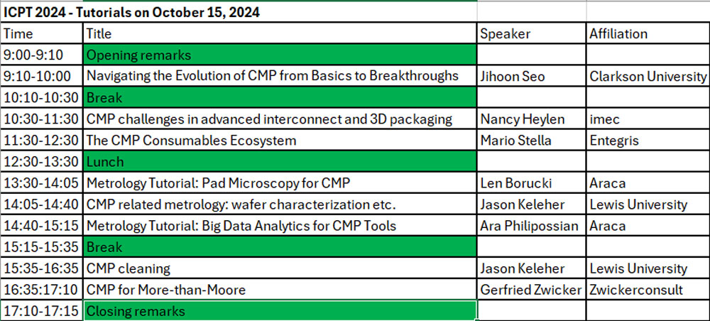
 

10:30 - 11:30 Nancy Heylen - CMP challenges in advanced interconnect and 3D packaging

Nancy Heylen, R&D team leader
IMEC, Belgium

Biography
Nancy Heylen, Ph.D. is an R&D team lead in the CMP group of the Unit Process and Module division at Imec in Belgium. She has been working at IMEC since March 1997 and within a timeframe of more than 25 years she has been mainly involved in the process development of metal CMP steps and post-CMP cleaning processes starting from the 0.35 μm down to the 2 nm technology node. The last few years she was, as a senior R&D engineer, mainly involved in the development of metal CMP process steps (Cu, Ta, Co, Mo, Ru, binary metal) for 3Di and nano interconnect technology. She has started a new role as R&D team lead of the CMPPMEC team in 2023.
She received her Ph.D. degree in Chemistry at the University of Leuven, Belgium in 1996.

CMP challenges in advanced interconnect and 3D packaging
The scaling of the device density in both logic and memory circuits entails the scaling of the interconnect line dimensions. Today, the characteristic dimensions of interconnects in state-of-the-art microelectronic chips approach 10 nm and will reach even smaller dimensions in the near future. In the nanointerconnect landscape scaling boosters like semidamascene approaches and the introduction of alternative metals (replacing Cu) enable future technology nodes. Resistance and reliability are improved by replacing Cu with elemental alternative metals, and recently, focus of forefront alternative metal research at IMEC has shifted to binary intermetallics. For nanointerconnect metal CMP is needed in all scaling approaches and boosters, leading to more stringent criteria and more challenges. 
Also For 3Di technology the 3D interconnect pitch is being reduced, enabling an increased device density and performance. In recent years, die-to-wafer (D2W) and wafer-to-wafer (W2W) hybrid bonding have become essential technologies in the development of electronic devices. The continuous scaling to finer pitches in direct W2W hybrid bonding requires continuous CMP R&D and process adaptation to meet the increasingly more stringent post-CMP nanotopography requirements for optimal bonding efficiency. 
For all technologies CMP process solutions consist of selecting optimal combinations of tool features, process conditions and consumables, considering many scaling challenges. 


11:30 - 12:30 Mario Stella - The CMP Consumables Ecosystem 

Mario Stella
Fab Technology Engineering Director at Entegris

Biography
For nearly 30 years, Mario has been involved in process engineering in the semiconductor industry – primarily focused on CMP, which is his passion. 
Having worked for integrated device manufacturing fabs, CMP equipment manufacturers and CMP consumables producers, Mario has acquired a thorough understanding of the multi-faceted CMP environment, which he now employs for the development of comprehensive consumable solutions for CMP’s various challenges, working closely with CMP users, and mentoring and training CMP engineers across multiple companies.

The CMP Consumables Ecosystem 
Let’s delve into the CMP Ecosystem and uncover what CMP chemicals and consumables are needed to make CMP equipment run and how these consumables influence your CMP performance.

13:30 - 14:05 Len Borucki - Pad Microscopy for CMP

Len Borucki
Araca Inc. CTO (ret.)

Biography
Len Borucki received B.S. and Ph.D. degrees in mathematics from Rensselaer Polytechnic Institute. After teaching mathematics and statistics at Lafayette College, he joined IBM in Burlington, Vermont, where he was the primary developer of the semiconductor process modeling tool FEDSS. Len then moved to Motorola in Phoenix, Arizona, where he became a Fellow of the Technical Staff and first worked on CMP. He subsequently ran his own company, Intelligent Planar, before joining Araca Incorporated as Chief Technology Officer.  Len has authored or co-authored numerous journal and proceedings papers and two book chapters and has several CMP patents. He is currently semi-retired and living in Oregon.

Metrology Tutorial: Pad Microscopy for CMP
CMP pad topography affects slurry transport, contact area, defectivity, friction, and material removal rates. This tutorial will discuss how to use confocal microscopy data to do a CMP-relevant pad surface characterization. This includes the pad surface height distribution and some simple related measures as well as functions such as the summit height distribution and summit curvature distribution. We also show how to use confocal microscopy to measure the contact area between the pad and wafer. By comparing topography, contact area images, and scanning electron microscopy images of the same area, we show that that pad surfaces are not always what you might expect from one type of image alone. For example, a confocal topography image may suggest conventional mechanical behavior while multiple image types may indicate a different type of behavior in which contact area and removal are dominated by conditioning debris, with observable consequences for a CMP process.
 

14:05 - 14:40 Jason Keleher - Challenges and Innovations for post-CMP Cleaning of Emerging Materials/Processes at Advanced Technology Nodes - Part 1: CMP related metrology

Dr. Jason J. Keleher
Professor and Chair of Chemistry, Lewis University 

Biography

Dr. Jason Keleher currently serves as Full Professor and Chair of the Department of Chemistry at Lewis University. He is also the Principal Investigator of the Keleher Research Group (KRG) (est. 2009). Dr. Keleher’s career began in 2004 as a Postdoc Research Scientist at Komag Inc. (Western Digital Inc.), where he developed slurry formulations for next-generation texturing processes for magnetic recording thin film media. Dr. Keleher then transitioned to Senior Research Scientist at Cabot Microelectronics Corporation (Entegris Inc.), where he provided a mechanistic understanding of chemical reactions at the nanoparticle/polymer/substrate interface. Currently, his group focuses on investigating the fundamental mechanisms behind CMP and post-CMP processes of emerging substrates via modulation of the redox environment. Their research has resulted in 50 publications, 25 U.S. patents, and over 400 presentations, as well as numerous funded collaborations with industry partners to advance fundamental understanding relevant to the semiconductor industry.

Challenges and Innovations for post-CMP Cleaning of Emerging Materials/Processes at Advanced Technology Nodes
Part1: CMP related metrology: Wafer characterization, etc.

This presentation will explore methods of substrate characterization metrology to evaluate the Chemical Mechanical Planarization (CMP) processes. The discussion will focus on techniques such as atomic force microscopy (AFM), scanning electron microscopy (SEM), green light/white light interferometry, ellipsometry, and bow and total thickness variation (TTV). A few case studies will show the correlation between fundamental polishing and cleaning mechanisms and output from wafer analysis using several techniques previously mentioned and discussed to provide critical insights into CMP process optimization.

14:40 - 15:15 Ara Philipossian - Big Data Analytics for CMP Tools

Ara Philipossian
Araca Inc. President and CEO

Biography
Dr. Philipossian is the Co-Founder, President and CEO of Araca Inc., the premier provider of services and equipment to the polishing and planarization industry worldwide. He received his BS, MS and PhD in Chemical Engineering from Tufts University in 1983, 1985 and 1992, respectively. He was a professor of Chemical Engineering at the University of Arizona from 2001 to 2021 where he held the Koshiyama Chair of Planarization. From 1992 to 2001, he was the Materials Technology Manager at Intel (Santa Clara, CA USA) responsible for development, characterization, implementation and sustaining of new and existing CMP and post-CMP cleaning consumables, low k dielectrics and electroplating chemicals. From 1986 to 1992, he worked at Digital Equipment (Hudson, MA USA) as a process development manager focusing on thermal silicon oxidation, diffusion, LPCVD of dielectric and gate electrodes, and wafer cleaning technology. Dr. Philipossian has authored 185 archival journal publications along with 210 conference proceedings articles. He holds 36 patents related to semiconductor processing and device fabrication.

Metrology Tutorial: Big Data Analytics for CMP Tools
Modern polishers used in high-volume-manufacturing are fitted with many high-frequency sensors for measuring key process parameters vs. polish time. These sensors generate and store 100s of millions of data points in a typical 1-minute run. If analyzed properly, such data can add to the planarization knowledge base and provide deep fundamental insight. This tutorial will show how (via a certain customized software package) big data gathering processes can be organized, analyzed, modeled, centralized and shared within various R&D sites in a company. The tutorial will also emphasize multi-variate filtering, relational plots, correlation analyses, ANOVA analyses and significance factor determinations, data animations. Furthermore, many other features will be demonstrated.
 

15:35 - 16:35 Jason Keleher - Challenges and Innovations for post-CMP Cleaning of Emerging Materials/Processes at Advanced Technology Nodes- Part 2: CMP Cleaning

Dr. Jason J. Keleher
Professor and Chair of Chemistry, Lewis University 

Biography

Dr. Jason Keleher currently serves as Full Professor and Chair of the Department of Chemistry at Lewis University. He is also the Principal Investigator of the Keleher Research Group (KRG) (est. 2009). Dr. Keleher’s career began in 2004 as a Postdoc Research Scientist at Komag Inc. (Western Digital Inc.), where he developed slurry formulations for next-generation texturing processes for magnetic recording thin film media. Dr. Keleher then transitioned to Senior Research Scientist at Cabot Microelectronics Corporation (Entegris Inc.), where he provided a mechanistic understanding of chemical reactions at the nanoparticle/polymer/substrate interface. Currently, his group focuses on investigating the fundamental mechanisms behind CMP and post-CMP processes of emerging substrates via modulation of the redox environment. Their research has resulted in 50 publications, 25 U.S. patents, and over 400 presentations, as well as numerous funded collaborations with industry partners to advance fundamental understanding relevant to the semiconductor industry.

Challenges and Innovations for post-CMP Cleaning of Emerging Materials/Processes at Advanced Technology Nodes
Part2: CMP Cleaning

As integrated circuit and logic device feature sizes approach the 3-nm node, limiting induced defectivity during the Chemical Mechanical Planarization (CMP) process (polishing and substrate cleaning) is paramount. The CMP/p-CMP processes cause defects that can be classified as mechanical (i.e., scratching), chemical (i.e., corrosion), or physiochemical (i.e., adsorbed contaminants) according to the interfacial mechanism of formation. This tutorial will address the following topics through a series of case studies highlighting the fundamental interfacial dynamics necessary for the rational design of advanced p-CMP cleaning processes. A survey of current p-CMP schemes (consumables and processing conditions) for metal, advanced STI, and emerging materials (SiC and GaN) will be presented. Specific emphasis will be placed on highlighting challenges for mitigating particle, corrosion, and residue defects.
 

16:35 - 17:10 Gerfried Zwicker - CMP for More-than-Moore

Gerfried Zwicker, zwickerconsult

Biography
Gerfried Zwicker studied physics at TU Berlin where he graduated on electroluminescence of II-VI semiconductors for his diploma. At the Fritz-Haber-Institute in Berlin he investigated surface properties of ZnO for his dissertation. He joined the Fraunhofer Institute for Microstructure Technology IMT in 1985, where he worked on CMOS Technology by using x-ray lithography with emphasis on reactive ion etching RIE. After moving to the Fraunhofer Institute for Silicon Technology ISIT in Itzehoe in 1995 he concentrated on Chemical Mechanical Polishing CMP and was responsible for CMP tool development, consumables evaluation and process adoption for MEMS and powerMOS applications.
Dr. Gerfried Zwicker is founder and organizer of the European CMP Users Meeting and was co-founder and member of the Executive Committee of ICPT. He is author/co-author of more than 50 publications and book contributions. After his retirement he offers his longtime experience in microelectronics as an independent consultant.

CMP for More-than-Moore
More-than-Moore applications like MEMS, analog, powerMOS, optoMEMS, packaging, bonding etc. require smooth and even surfaces which can only be achieved by chemical-mechanical polishing CMP. Due to increasing mass fabrication of these devices multiple CMP processes must fulfill the same specifications as those for microelectronics manufacturing. Several typical examples of the application of CMP for More-than-Moore will be given.